🚚 Free Worldwide Shipping on All Orders!Shop Now

InP-(VGF- Grown) (111)B S doped, 2"x0.35mm wafer, 1sp
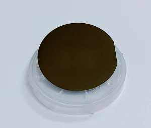
- InP single crystal wafer
- Growing Method: VGF
- Orientation: (111)B
- Size: 2" diameter x 0.35 mm
- Doping: S- doped
- Conducting type: S-C-N
- Polish: one side polished
- Resistivity: (1.26-1.40)x10^-3 ohm.cm
- Mobility: (1540-1650) cm^2/v.s
- EPD: N/A
- Carrier Concentration: (2.71-3.24) x10^18 /cm^3
- Surface Roughness: <4 nm
- EPI ready surface and packing
$488.25
Original: $1,395.00
-65%InP-(VGF- Grown) (111)B S doped, 2"x0.35mm wafer, 1sp—
$1,395.00
$488.25InP-(VGF- Grown) (111)B S doped, 2"x0.35mm wafer, 1sp
- InP single crystal wafer
- Growing Method: VGF
- Orientation: (111)B
- Size: 2" diameter x 0.35 mm
- Doping: S- doped
- Conducting type: S-C-N
- Polish: one side polished
- Resistivity: (1.26-1.40)x10^-3 ohm.cm
- Mobility: (1540-1650) cm^2/v.s
- EPD: N/A
- Carrier Concentration: (2.71-3.24) x10^18 /cm^3
- Surface Roughness: <4 nm
- EPI ready surface and packing
Product Information
Product Information
Shipping & Returns
Shipping & Returns
Description
- InP single crystal wafer
- Growing Method: VGF
- Orientation: (111)B
- Size: 2" diameter x 0.35 mm
- Doping: S- doped
- Conducting type: S-C-N
- Polish: one side polished
- Resistivity: (1.26-1.40)x10^-3 ohm.cm
- Mobility: (1540-1650) cm^2/v.s
- EPD: N/A
- Carrier Concentration: (2.71-3.24) x10^18 /cm^3
- Surface Roughness: <4 nm
- EPI ready surface and packing