🚚 Free Worldwide Shipping on All Orders!Shop Now

InAs (100), P Type, Zn doped 2" dia x 0.5 mm, one side polished - IAZna50D05C1US5
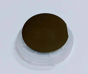
2" InAs wafer (P type)
- 2" InAs wafer
- P Type, Zn doped
- Size: 2" dia x0. 5 mm +/-20 microns
- Orientation: <100> +/-0.50
- Polishing: one-side polishd
- Packing: in 1000 class clean room with wafer container
Properties
- Growth method LEC
- Orientation (100) +/- 0.5 o
- Orientation Flat <110> <-110>
- Doping Zn doped
- Conductivity type P type
- Carrier Concentration (3-7)E17/ cm3
- Mobility 100-500 cm2/V.S
- EPD <10000 / cm 2
$488.25
Original: $1,395.00
-65%InAs (100), P Type, Zn doped 2" dia x 0.5 mm, one side polished - IAZna50D05C1US5—
$1,395.00
$488.25InAs (100), P Type, Zn doped 2" dia x 0.5 mm, one side polished - IAZna50D05C1US5
2" InAs wafer (P type)
- 2" InAs wafer
- P Type, Zn doped
- Size: 2" dia x0. 5 mm +/-20 microns
- Orientation: <100> +/-0.50
- Polishing: one-side polishd
- Packing: in 1000 class clean room with wafer container
Properties
- Growth method LEC
- Orientation (100) +/- 0.5 o
- Orientation Flat <110> <-110>
- Doping Zn doped
- Conductivity type P type
- Carrier Concentration (3-7)E17/ cm3
- Mobility 100-500 cm2/V.S
- EPD <10000 / cm 2
Product Information
Product Information
Shipping & Returns
Shipping & Returns
Description
2" InAs wafer (P type)
- 2" InAs wafer
- P Type, Zn doped
- Size: 2" dia x0. 5 mm +/-20 microns
- Orientation: <100> +/-0.50
- Polishing: one-side polishd
- Packing: in 1000 class clean room with wafer container
Properties
- Growth method LEC
- Orientation (100) +/- 0.5 o
- Orientation Flat <110> <-110>
- Doping Zn doped
- Conductivity type P type
- Carrier Concentration (3-7)E17/ cm3
- Mobility 100-500 cm2/V.S
- EPD <10000 / cm 2