🚚 Free Worldwide Shipping on All Orders!Shop Now
GaAs Wafer, Growing Method: VGF, (100) undoped Semi-Insulated 2"D x0.5 mm, 1SP
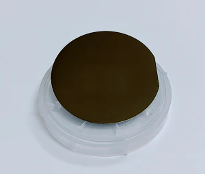
- GaAs single crystal wafer
- Growing Method: VGF
- Orientation: (100)+/-0.5 degree
- Size: 2" dia x 0.5mm
- Polishing: single side polished
- Doping: un- doped
- Conductor type: Semi-insulating
- Ra(Average Roughness) : < 0.4 nm
- Mobility: 4470-6540 cm^2/V.S
- Resistivity: (0.96-5.34) x 10^8 ohm.cm
- EPD: <5000cm^2
- EPI ready surface and packing
$204.75
Original: $585.00
-65%GaAs Wafer, Growing Method: VGF, (100) undoped Semi-Insulated 2"D x0.5 mm, 1SP—
$585.00
$204.75GaAs Wafer, Growing Method: VGF, (100) undoped Semi-Insulated 2"D x0.5 mm, 1SP
- GaAs single crystal wafer
- Growing Method: VGF
- Orientation: (100)+/-0.5 degree
- Size: 2" dia x 0.5mm
- Polishing: single side polished
- Doping: un- doped
- Conductor type: Semi-insulating
- Ra(Average Roughness) : < 0.4 nm
- Mobility: 4470-6540 cm^2/V.S
- Resistivity: (0.96-5.34) x 10^8 ohm.cm
- EPD: <5000cm^2
- EPI ready surface and packing
Product Information
Product Information
Shipping & Returns
Shipping & Returns
Description
- GaAs single crystal wafer
- Growing Method: VGF
- Orientation: (100)+/-0.5 degree
- Size: 2" dia x 0.5mm
- Polishing: single side polished
- Doping: un- doped
- Conductor type: Semi-insulating
- Ra(Average Roughness) : < 0.4 nm
- Mobility: 4470-6540 cm^2/V.S
- Resistivity: (0.96-5.34) x 10^8 ohm.cm
- EPD: <5000cm^2
- EPI ready surface and packing