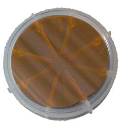
GaP wafer, S doped, (100), 5 x 5 x 0.5 mm, 1sp
- (GaP single crystal wafer
- Size:5mmx5mmx0.5mm
- Doping: S-doped,
- Conducting type: N-type
- Orientation: (100)+_30'
- Polished: One side polished.
- Surface finish (RMS or Ra) : < 8A
Typical Physical Properties |
||
Crystal Structure |
Cubic. a =5.4505 ?/FONT> |
|
Growth Method |
CZ (LEC) |
|
Density |
4.13 g/cm3 |
|
Melt Point |
1480 oC |
|
Thermal Expansion |
5.3 x10⁻⁶ / oC |
|
Dopant |
S doped |
undoped |
Crystal growth axis |
<111> or <100> |
<100> or <111> |
Conducting Type |
N |
N |
Carrier Concentration |
(2 ~ 12) x1017 /cm3 |
4 ~ 6 x10¹⁶ /cm3 |
Resistivity |
~ 0.03ohm-cm |
~ 0.3 ohm-cm |
EPD |
< 3x10⁵ |
< 3x10⁵ |
|
|
|
|
|
Other Crystal wafer A-Z |
Plasma Cleaner |
Wafer Containers |
Dicing saw |
Film Coater |
Product Information
Product Information
Shipping & Returns
Shipping & Returns
Description
- (GaP single crystal wafer
- Size:5mmx5mmx0.5mm
- Doping: S-doped,
- Conducting type: N-type
- Orientation: (100)+_30'
- Polished: One side polished.
- Surface finish (RMS or Ra) : < 8A
Typical Physical Properties |
||
Crystal Structure |
Cubic. a =5.4505 ?/FONT> |
|
Growth Method |
CZ (LEC) |
|
Density |
4.13 g/cm3 |
|
Melt Point |
1480 oC |
|
Thermal Expansion |
5.3 x10⁻⁶ / oC |
|
Dopant |
S doped |
undoped |
Crystal growth axis |
<111> or <100> |
<100> or <111> |
Conducting Type |
N |
N |
Carrier Concentration |
(2 ~ 12) x1017 /cm3 |
4 ~ 6 x10¹⁶ /cm3 |
Resistivity |
~ 0.03ohm-cm |
~ 0.3 ohm-cm |
EPD |
< 3x10⁵ |
< 3x10⁵ |
|
|
|
|
|
Other Crystal wafer A-Z |
Plasma Cleaner |
Wafer Containers |
Dicing saw |
Film Coater |