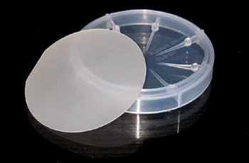
AlN Template on 4" Silicon (Si <111>, P type, B-doped) 4"x 500 nm - FmAlNonSiBc101D05C1FT500nmUS
AlN Template on 4" Silicon (Si <111>, P type, B-doped) 4"x 500 nm - FmAlNonSiBc101D05C1FT500nmUS
AlN Template on Silicon is made by a PVDNC method. AlN template on Silicon is a cost effective way to replace AlN single crystal substrate.
Specifications
- Useful area: 90%
-
Nominal AlN thickness: 500nm ±10%, one side coated, undoped AlN film
-
Front Surface: as-grown
-
Back surface: silicon as received
-
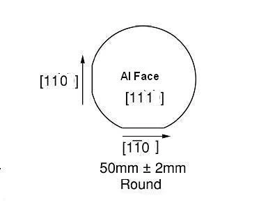
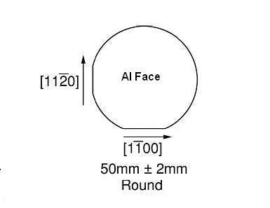
AlN orientation: C-plane (00.1)
-
Macro Defect Density: <10/cm^2
-
Wafer base: Silicon [111] P type, 4" dia x0.5 mm, , one side polished,R<5 ohm.cm
- For Standard Cleaning of AlN template, please click here.
- Please click here to see technical data for AlN template.
- For physical property sheet of AlN Template, please click here.
Related data
-
AlN MSDS
Related Products
 |
|
|
|
|
|
|
Thin Films A-Z |
Crystal wafer A-Z |
Plasma Cleaner |
Wafer Containers |
Dicing saw |
Film Coater |
Original: $1,118.00
-65%$1,118.00
$391.30AlN Template on 4" Silicon (Si <111>, P type, B-doped) 4"x 500 nm - FmAlNonSiBc101D05C1FT500nmUS
AlN Template on Silicon is made by a PVDNC method. AlN template on Silicon is a cost effective way to replace AlN single crystal substrate.
Specifications
- Useful area: 90%
-
Nominal AlN thickness: 500nm ±10%, one side coated, undoped AlN film
-
Front Surface: as-grown
-
Back surface: silicon as received
-
AlN orientation: C-plane (00.1)
-
Macro Defect Density: <10/cm^2
-
Wafer base: Silicon [111] P type, 4" dia x0.5 mm, , one side polished,R<5 ohm.cm
- For Standard Cleaning of AlN template, please click here.
- Please click here to see technical data for AlN template.
- For physical property sheet of AlN Template, please click here.
Related data
-
AlN MSDS
Related Products
|
|
|
|
|
|
|
Thin Films A-Z |
Crystal wafer A-Z |
Plasma Cleaner |
Wafer Containers |
Dicing saw |
Film Coater |
Product Information
Product Information
Shipping & Returns
Shipping & Returns
Description
AlN Template on Silicon is made by a PVDNC method. AlN template on Silicon is a cost effective way to replace AlN single crystal substrate.
Specifications
- Useful area: 90%
-
Nominal AlN thickness: 500nm ±10%, one side coated, undoped AlN film
-
Front Surface: as-grown
-
Back surface: silicon as received
-
AlN orientation: C-plane (00.1)
-
Macro Defect Density: <10/cm^2
-
Wafer base: Silicon [111] P type, 4" dia x0.5 mm, , one side polished,R<5 ohm.cm
- For Standard Cleaning of AlN template, please click here.
- Please click here to see technical data for AlN template.
- For physical property sheet of AlN Template, please click here.
Related data
-
AlN MSDS
Related Products
|
|
|
|
|
|
|
Thin Films A-Z |
Crystal wafer A-Z |
Plasma Cleaner |
Wafer Containers |
Dicing saw |
Film Coater |