🚚 Free Worldwide Shipping on All Orders!Shop Now

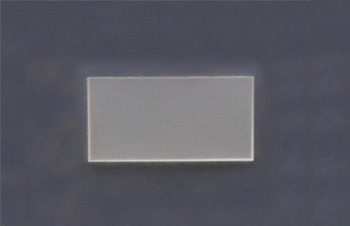
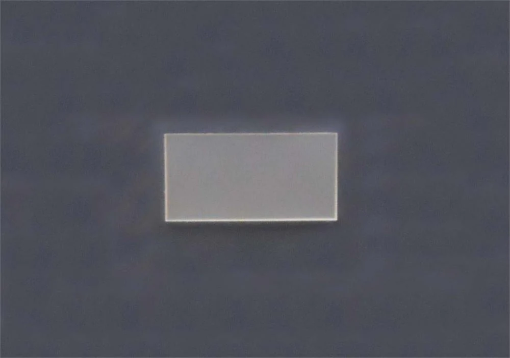
Al2O3 - Sapphire Wafer, C-plane (0001), 2"dia x 0.5mm 2SP - ALC50D05C2
Features:
- Sapphire (single crystal of Al2O3 ) is being used extensively as a substrate for III-V nitrides and for many other epitaxial films
- Orientation: C-axis[0001]( +/-0.3 Deg) with Standard Flat
- Diameter: 2" +/- 0.3mm
- Thickness: 500um +/- 25 um
- Major Flat: A-axis[11-20]+/-0.2o
- Surface Finish: Front sides: Epi- polished Ra<0.5nm (by AFM)
- Back side: Epi- polished , <0.5nm(by AFM)
- TTV: < 10um
- Polished surface: Two side epi polished by special CMP technology
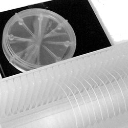
- Package: Each wafer is packed in 1000 class clean room
Typical Properties:
-
Crystal Structure: Hexagonal. a=4.758 Angstroms c=12.99 Angstroms
-
Melting Point: 2040 degree C
-
Density: 3.97 gram/cm2
-
Growth Technique: CZ
-
Crystal Purity: >99.99%
-
Hardness: 9 ( mohs)
-
Thermal Expansion: 7.5x10⁻⁶ (/ oC)
-
Thermal Conductivity: 46.06 @ 0 oC, 25.12 @ 100 oC, 12.56 @ 400 oC ( W/(m.K) )
-
Dielectric Constant: ~ 9.4 @300K at A axis ~ 11.58@ 300K at C axis
-
Loss Tangent at 10 GHz: < 2x10⁻⁵ at A axis, <5 x10⁻⁵ at C axis
Related Products
|
Other Sapphire |
GaN |
AlN template |
ZnO |
|
|
|
|
|
|
Diamond Scriber |
Vacuum Pen |
Wafer Containers |
Film Coaters |
|
|
|
|
$17.48
Original: $49.95
-65%Al2O3 - Sapphire Wafer, C-plane (0001), 2"dia x 0.5mm 2SP - ALC50D05C2—
$49.95
$17.48Al2O3 - Sapphire Wafer, C-plane (0001), 2"dia x 0.5mm 2SP - ALC50D05C2
Features:
- Sapphire (single crystal of Al2O3 ) is being used extensively as a substrate for III-V nitrides and for many other epitaxial films
- Orientation: C-axis[0001]( +/-0.3 Deg) with Standard Flat
- Diameter: 2" +/- 0.3mm
- Thickness: 500um +/- 25 um
- Major Flat: A-axis[11-20]+/-0.2o
- Surface Finish: Front sides: Epi- polished Ra<0.5nm (by AFM)
- Back side: Epi- polished , <0.5nm(by AFM)
- TTV: < 10um
- Polished surface: Two side epi polished by special CMP technology
- Package: Each wafer is packed in 1000 class clean room
Typical Properties:
-
Crystal Structure: Hexagonal. a=4.758 Angstroms c=12.99 Angstroms
-
Melting Point: 2040 degree C
-
Density: 3.97 gram/cm2
-
Growth Technique: CZ
-
Crystal Purity: >99.99%
-
Hardness: 9 ( mohs)
-
Thermal Expansion: 7.5x10⁻⁶ (/ oC)
-
Thermal Conductivity: 46.06 @ 0 oC, 25.12 @ 100 oC, 12.56 @ 400 oC ( W/(m.K) )
-
Dielectric Constant: ~ 9.4 @300K at A axis ~ 11.58@ 300K at C axis
-
Loss Tangent at 10 GHz: < 2x10⁻⁵ at A axis, <5 x10⁻⁵ at C axis
Related Products
|
Other Sapphire |
GaN |
AlN template |
ZnO |
|
|
|
|
|
|
Diamond Scriber |
Vacuum Pen |
Wafer Containers |
Film Coaters |
|
|
|
|
Product Information
Product Information
Shipping & Returns
Shipping & Returns
Description
Features:
- Sapphire (single crystal of Al2O3 ) is being used extensively as a substrate for III-V nitrides and for many other epitaxial films
- Orientation: C-axis[0001]( +/-0.3 Deg) with Standard Flat
- Diameter: 2" +/- 0.3mm
- Thickness: 500um +/- 25 um
- Major Flat: A-axis[11-20]+/-0.2o
- Surface Finish: Front sides: Epi- polished Ra<0.5nm (by AFM)
- Back side: Epi- polished , <0.5nm(by AFM)
- TTV: < 10um
- Polished surface: Two side epi polished by special CMP technology
- Package: Each wafer is packed in 1000 class clean room
Typical Properties:
-
Crystal Structure: Hexagonal. a=4.758 Angstroms c=12.99 Angstroms
-
Melting Point: 2040 degree C
-
Density: 3.97 gram/cm2
-
Growth Technique: CZ
-
Crystal Purity: >99.99%
-
Hardness: 9 ( mohs)
-
Thermal Expansion: 7.5x10⁻⁶ (/ oC)
-
Thermal Conductivity: 46.06 @ 0 oC, 25.12 @ 100 oC, 12.56 @ 400 oC ( W/(m.K) )
-
Dielectric Constant: ~ 9.4 @300K at A axis ~ 11.58@ 300K at C axis
-
Loss Tangent at 10 GHz: < 2x10⁻⁵ at A axis, <5 x10⁻⁵ at C axis
Related Products
|
Other Sapphire |
GaN |
AlN template |
ZnO |
|
|
|
|
|
|
Diamond Scriber |
Vacuum Pen |
Wafer Containers |
Film Coaters |
|
|
|
|