🚚 Free Worldwide Shipping on All Orders!Shop Now
HomeStore
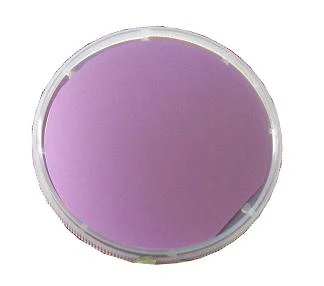
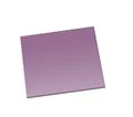
Thermal Oxide Wafer: 285nm SiO2 on Si (100), 10 x 10 x 0.5 mm, N type ,P-doped 1SP, R:1-10 ohm.cm
Thermal Oxide Wafer: 285nm SiO2 on Si (100), 10 x 10 x 0.5 mm, N type ,P-doped 1SP, R:1-10 ohm.cm
Thermal oxide Layer
- SiO2 layer on Silicon wafer
- Oxide layer thickness: 285 nm ( 500A) +/-10%
- Refractive index - 1.455
Silicon Wafer Specifications:
- Conductive type: N-type/ P-dped
- Resistivity: 1-10 ohm.cm (If you would like to measure the resistivity accurately,
please order our Portable 4 Probe Resistivity Testing Instrument.) - Size: 10 x 10 x 0.5 mm
- Orientation: (100) +/- 1o
- Polish: one side polished
- Surface roughness, Ra: < 5A (RMS)
Related Products
 |
|
|
|
|
|
Thin Films A-Z |
Crystal wafer A-Z |
Plasma Cleaner |
Wafer Containers |
Dicing saw |
Film Coater |
$10.48
Original: $29.95
-65%Thermal Oxide Wafer: 285nm SiO2 on Si (100), 10 x 10 x 0.5 mm, N type ,P-doped 1SP, R:1-10 ohm.cm—
$29.95
$10.48Thermal Oxide Wafer: 285nm SiO2 on Si (100), 10 x 10 x 0.5 mm, N type ,P-doped 1SP, R:1-10 ohm.cm
Thermal oxide Layer
- SiO2 layer on Silicon wafer
- Oxide layer thickness: 285 nm ( 500A) +/-10%
- Refractive index - 1.455
Silicon Wafer Specifications:
- Conductive type: N-type/ P-dped
- Resistivity: 1-10 ohm.cm (If you would like to measure the resistivity accurately,
please order our Portable 4 Probe Resistivity Testing Instrument.) - Size: 10 x 10 x 0.5 mm
- Orientation: (100) +/- 1o
- Polish: one side polished
- Surface roughness, Ra: < 5A (RMS)
Related Products
|
|
|
|
|
|
Thin Films A-Z |
Crystal wafer A-Z |
Plasma Cleaner |
Wafer Containers |
Dicing saw |
Film Coater |
Product Information
Product Information
Shipping & Returns
Shipping & Returns
Description
Thermal oxide Layer
- SiO2 layer on Silicon wafer
- Oxide layer thickness: 285 nm ( 500A) +/-10%
- Refractive index - 1.455
Silicon Wafer Specifications:
- Conductive type: N-type/ P-dped
- Resistivity: 1-10 ohm.cm (If you would like to measure the resistivity accurately,
please order our Portable 4 Probe Resistivity Testing Instrument.) - Size: 10 x 10 x 0.5 mm
- Orientation: (100) +/- 1o
- Polish: one side polished
- Surface roughness, Ra: < 5A (RMS)
Related Products
|
|
|
|
|
|
Thin Films A-Z |
Crystal wafer A-Z |
Plasma Cleaner |
Wafer Containers |
Dicing saw |
Film Coater |