🚚 Free Worldwide Shipping on All Orders!Shop Now

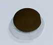
InSb (111)- B 2" dia x 0.45 mm, Te-doped, N type, 1 side(Sb) polished
2" InSb wafer (N type, Te-doped)
- Size: 2" dia x 0.45-0.5mm thick with thickness tolerance +/- 25 um
- Orientation <111>B +/-0.5o
- Polishing: one-side side(Sb) polishd ( back side etched )
- Packing: Sealed under nitrogen with single wafer comtainer in 1000 class clean room
Properties
- Growth method LEC
- Orientation <111>B +/- 0.5o
- Doping Te-doped
- Conductivity type N type
- Carrier Concentration (5.0E17 - 2.0E18) cm-3 @77K
- Mobility 24,000-34,000 cm2/Vs
- EPD <1.0 E+3 / cm -2
$567.00
Original: $1,620.00
-65%InSb (111)- B 2" dia x 0.45 mm, Te-doped, N type, 1 side(Sb) polished—
$1,620.00
$567.00InSb (111)- B 2" dia x 0.45 mm, Te-doped, N type, 1 side(Sb) polished
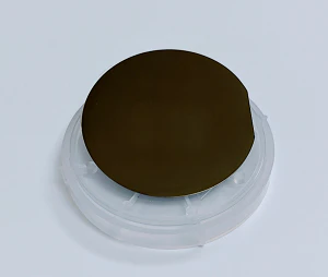
2" InSb wafer (N type, Te-doped)
- Size: 2" dia x 0.45-0.5mm thick with thickness tolerance +/- 25 um
- Orientation <111>B +/-0.5o
- Polishing: one-side side(Sb) polishd ( back side etched )
- Packing: Sealed under nitrogen with single wafer comtainer in 1000 class clean room
Properties
- Growth method LEC
- Orientation <111>B +/- 0.5o
- Doping Te-doped
- Conductivity type N type
- Carrier Concentration (5.0E17 - 2.0E18) cm-3 @77K
- Mobility 24,000-34,000 cm2/Vs
- EPD <1.0 E+3 / cm -2
Product Information
Product Information
Shipping & Returns
Shipping & Returns
Description
2" InSb wafer (N type, Te-doped)
- Size: 2" dia x 0.45-0.5mm thick with thickness tolerance +/- 25 um
- Orientation <111>B +/-0.5o
- Polishing: one-side side(Sb) polishd ( back side etched )
- Packing: Sealed under nitrogen with single wafer comtainer in 1000 class clean room
Properties
- Growth method LEC
- Orientation <111>B +/- 0.5o
- Doping Te-doped
- Conductivity type N type
- Carrier Concentration (5.0E17 - 2.0E18) cm-3 @77K
- Mobility 24,000-34,000 cm2/Vs
- EPD <1.0 E+3 / cm -2