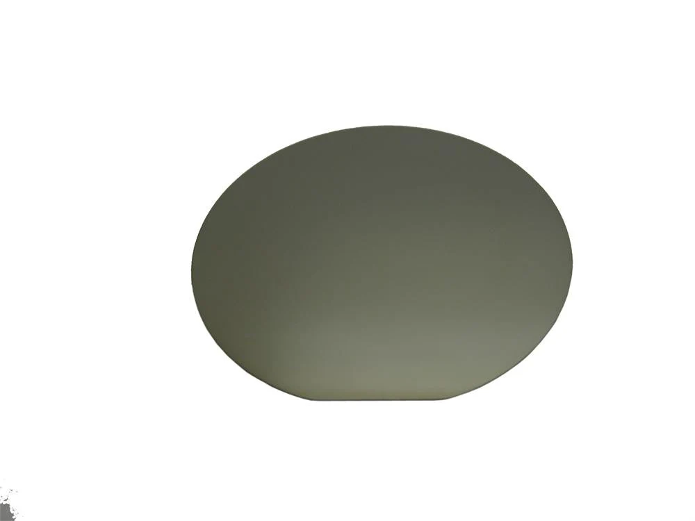
2" dia. InGaAs EPI Film on InP (SI) (100) Depositied by MOCVD ( InP:Fe) 2" dia x0.35mm,2sp,Film:750 nm
2" dia. InGaAs EPI Film on InP (SI) (100) Depositied by MOCVD ( InP:Fe) 2" dia x0.35mm,2sp,Film:750 nm
2" dia. wafer InGaAs EPI on InP (Semi-insulating)(100) by MOCVD deposition
Substrate:
- InP Orientation: (100)
- Doped with Fe, Semi-Insulating
- Wafer size: 2" diameter x 0.35 mm
- Both sides polished
EPI Film :
- Lattice matched In/Ga alloy layer of N-type InGaAs(undoped)
- Film Thickness :0.75 um (+/- 20%)
- Roughness of epi-layer is close to 1 mono-layer (ML)
- One the back side we can expect some deposits and we can't guarantee the same quality (roughness) as in the case of active layer surface.
EPI ready surface and packing
Typical Properties
Dopant |
Type |
Carrier Concentration ( cm-3) |
Mobility ( cm2/V.Sec) |
Resistivity ( ohm-cm ) |
EPD (cm-2) |
Undoped |
N |
7.5-9.5 x10¹⁵ |
4300-4400 |
1.6E-1-4.5E-1 |
<5000 |
Sn |
N |
0.5 ~1.0 x10¹⁸ 0.5 ~1.0 x10¹⁸ |
200 ~ 2400 1500 ~ 2000 |
0.001 ~ 0.002 0.0025~0.007 |
3~5 x10⁴ |
Zn |
P |
0.8 ~ 2.0 x10¹⁸ 2.5 ~ 4.0 x10¹⁸ |
2500 ~ 3500 1300 ~ 1600 |
0.0025 ~ 0.006 |
1~ 3 x10⁴ |
Fe |
Semi-Insulating |
N/A |
1550-1640 |
(2.1-2.7) x107 | <5000 |
Related Products
 |
|
|
|
|
|
Thin Films A-Z |
Crystal wafer A-Z |
Plasma Cleaner |
Wafer Containers |
Dicing saw |
Film Coater |
Original: $1,999.00
-65%$1,999.00
$699.652" dia. InGaAs EPI Film on InP (SI) (100) Depositied by MOCVD ( InP:Fe) 2" dia x0.35mm,2sp,Film:750 nm
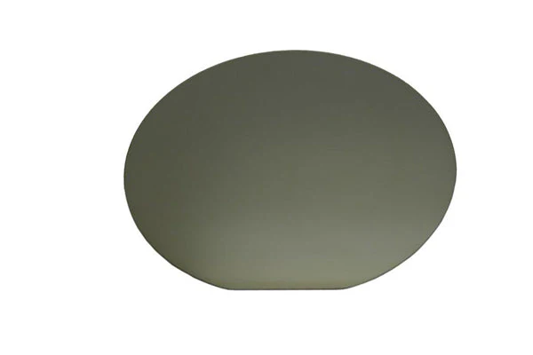
2" dia. wafer InGaAs EPI on InP (Semi-insulating)(100) by MOCVD deposition
Substrate:
- InP Orientation: (100)
- Doped with Fe, Semi-Insulating
- Wafer size: 2" diameter x 0.35 mm
- Both sides polished
EPI Film :
- Lattice matched In/Ga alloy layer of N-type InGaAs(undoped)
- Film Thickness :0.75 um (+/- 20%)
- Roughness of epi-layer is close to 1 mono-layer (ML)
- One the back side we can expect some deposits and we can't guarantee the same quality (roughness) as in the case of active layer surface.
EPI ready surface and packing
Typical Properties
Dopant |
Type |
Carrier Concentration ( cm-3) |
Mobility ( cm2/V.Sec) |
Resistivity ( ohm-cm ) |
EPD (cm-2) |
Undoped |
N |
7.5-9.5 x10¹⁵ |
4300-4400 |
1.6E-1-4.5E-1 |
<5000 |
Sn |
N |
0.5 ~1.0 x10¹⁸ 0.5 ~1.0 x10¹⁸ |
200 ~ 2400 1500 ~ 2000 |
0.001 ~ 0.002 0.0025~0.007 |
3~5 x10⁴ |
Zn |
P |
0.8 ~ 2.0 x10¹⁸ 2.5 ~ 4.0 x10¹⁸ |
2500 ~ 3500 1300 ~ 1600 |
0.0025 ~ 0.006 |
1~ 3 x10⁴ |
Fe |
Semi-Insulating |
N/A |
1550-1640 |
(2.1-2.7) x107 | <5000 |
Related Products
|
|
|
|
|
|
Thin Films A-Z |
Crystal wafer A-Z |
Plasma Cleaner |
Wafer Containers |
Dicing saw |
Film Coater |
Product Information
Product Information
Shipping & Returns
Shipping & Returns
Description
2" dia. wafer InGaAs EPI on InP (Semi-insulating)(100) by MOCVD deposition
Substrate:
- InP Orientation: (100)
- Doped with Fe, Semi-Insulating
- Wafer size: 2" diameter x 0.35 mm
- Both sides polished
EPI Film :
- Lattice matched In/Ga alloy layer of N-type InGaAs(undoped)
- Film Thickness :0.75 um (+/- 20%)
- Roughness of epi-layer is close to 1 mono-layer (ML)
- One the back side we can expect some deposits and we can't guarantee the same quality (roughness) as in the case of active layer surface.
EPI ready surface and packing
Typical Properties
Dopant |
Type |
Carrier Concentration ( cm-3) |
Mobility ( cm2/V.Sec) |
Resistivity ( ohm-cm ) |
EPD (cm-2) |
Undoped |
N |
7.5-9.5 x10¹⁵ |
4300-4400 |
1.6E-1-4.5E-1 |
<5000 |
Sn |
N |
0.5 ~1.0 x10¹⁸ 0.5 ~1.0 x10¹⁸ |
200 ~ 2400 1500 ~ 2000 |
0.001 ~ 0.002 0.0025~0.007 |
3~5 x10⁴ |
Zn |
P |
0.8 ~ 2.0 x10¹⁸ 2.5 ~ 4.0 x10¹⁸ |
2500 ~ 3500 1300 ~ 1600 |
0.0025 ~ 0.006 |
1~ 3 x10⁴ |
Fe |
Semi-Insulating |
N/A |
1550-1640 |
(2.1-2.7) x107 | <5000 |
Related Products
|
|
|
|
|
|
Thin Films A-Z |
Crystal wafer A-Z |
Plasma Cleaner |
Wafer Containers |
Dicing saw |
Film Coater |