🚚 Free Worldwide Shipping on All Orders!Shop Now

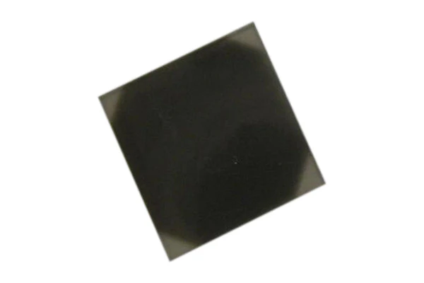
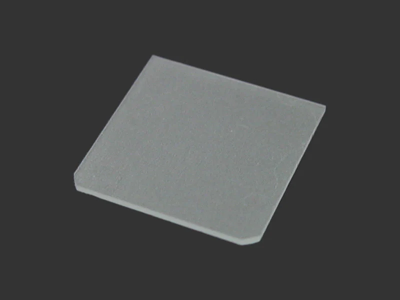
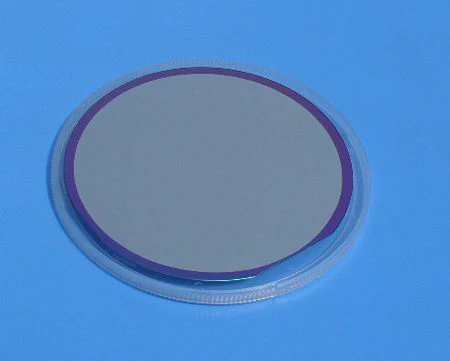
YBCO Thin Film 500nm ( two sides ) on Al2O3(R-plane), 10x10x0.5 mm
Epitaxial YBCO HTS Thin Film Up to 3" ( 75 mm )
MTI Corp joins with several research institutes around the world, to finally make high Tc superconducting
epitaxial thin film commercially available at an affordable price. MTI supplies high quality double side epitaxial
thin film up to 3" diameter on LaAlO3, LSAT, Al2O3 and SrTiO3 single crystal substrate by a unique technology.
This will make YBCO thin film available at very low cost. Researchers don't need to grow thin film any more, but concentrate their talent on HTSC film related devices, such as microwave filter for wireless and HTSC Squid.
Main Specifications of HTS Film
Epitaxial thin Film Composition |
<100> YBCO |
Film dimensionboth for one side or double side film |
YBCO / LaAlO3 10x10 mm ~ 3" dia.YBCO / LSAT 10x10 mm ~ 2" dia.YBCO / Al2O3 10x10 mm ~3" diaYBCO / STO 10x10 mm ~ 1" dia. |
Epitaxial FWHM |
< 0.2 o |
Critical Transition Temperature Tc |
90 K+/-5% |
Transition Temp. range ΔTc |
< 0.5 K |
Critical Current Jc |
2~3 MA/cm2 @ 77K 0T |
Surface Resistivity Rs |
< 1 m Ohm @ 10 GHz, 77K, 0T |
Thin film thickness |
100-500nm |
Uniformity for 2" wafer |
Thickness 300- 400 nmTc 86K-90KJc 3 +/-0.5 MA/cm2 @ 80% wafer center.
Note:
|
Package |
Sealed in Vacuum in a plastic box and bag. |
 |
 |
Double side 3" YBCO film on LaAlO3 Jc Uniformity measured FZK XRD pattern of Epi YBCO Film on LAO
Note: YBCO is very sensitive to moisture, and must be stored in desiccator box.
Related Products
 |
|
|
|
 |
|
|
Thin Films A-Z |
Crystal wafer A-Z |
Plasma Cleaner |
Wafer Containers |
Vacuum Storage Chambers |
Dicing saw |
Film Coater |
$120.75
Original: $345.00
-65%YBCO Thin Film 500nm ( two sides ) on Al2O3(R-plane), 10x10x0.5 mm—
$345.00
$120.75YBCO Thin Film 500nm ( two sides ) on Al2O3(R-plane), 10x10x0.5 mm
Epitaxial YBCO HTS Thin Film Up to 3" ( 75 mm )
MTI Corp joins with several research institutes around the world, to finally make high Tc superconducting
epitaxial thin film commercially available at an affordable price. MTI supplies high quality double side epitaxial
thin film up to 3" diameter on LaAlO3, LSAT, Al2O3 and SrTiO3 single crystal substrate by a unique technology.
This will make YBCO thin film available at very low cost. Researchers don't need to grow thin film any more, but concentrate their talent on HTSC film related devices, such as microwave filter for wireless and HTSC Squid.
Main Specifications of HTS Film
Epitaxial thin Film Composition |
<100> YBCO |
Film dimensionboth for one side or double side film |
YBCO / LaAlO3 10x10 mm ~ 3" dia.YBCO / LSAT 10x10 mm ~ 2" dia.YBCO / Al2O3 10x10 mm ~3" diaYBCO / STO 10x10 mm ~ 1" dia. |
Epitaxial FWHM |
< 0.2 o |
Critical Transition Temperature Tc |
90 K+/-5% |
Transition Temp. range ΔTc |
< 0.5 K |
Critical Current Jc |
2~3 MA/cm2 @ 77K 0T |
Surface Resistivity Rs |
< 1 m Ohm @ 10 GHz, 77K, 0T |
Thin film thickness |
100-500nm |
Uniformity for 2" wafer |
Thickness 300- 400 nmTc 86K-90KJc 3 +/-0.5 MA/cm2 @ 80% wafer center.
Note:
|
Package |
Sealed in Vacuum in a plastic box and bag. |
|
|
Double side 3" YBCO film on LaAlO3 Jc Uniformity measured FZK XRD pattern of Epi YBCO Film on LAO
Note: YBCO is very sensitive to moisture, and must be stored in desiccator box.
Related Products
|
|
|
|
|
|
|
Thin Films A-Z |
Crystal wafer A-Z |
Plasma Cleaner |
Wafer Containers |
Vacuum Storage Chambers |
Dicing saw |
Film Coater |
Product Information
Product Information
Shipping & Returns
Shipping & Returns
Description
Epitaxial YBCO HTS Thin Film Up to 3" ( 75 mm )
MTI Corp joins with several research institutes around the world, to finally make high Tc superconducting
epitaxial thin film commercially available at an affordable price. MTI supplies high quality double side epitaxial
thin film up to 3" diameter on LaAlO3, LSAT, Al2O3 and SrTiO3 single crystal substrate by a unique technology.
This will make YBCO thin film available at very low cost. Researchers don't need to grow thin film any more, but concentrate their talent on HTSC film related devices, such as microwave filter for wireless and HTSC Squid.
Main Specifications of HTS Film
Epitaxial thin Film Composition |
<100> YBCO |
Film dimensionboth for one side or double side film |
YBCO / LaAlO3 10x10 mm ~ 3" dia.YBCO / LSAT 10x10 mm ~ 2" dia.YBCO / Al2O3 10x10 mm ~3" diaYBCO / STO 10x10 mm ~ 1" dia. |
Epitaxial FWHM |
< 0.2 o |
Critical Transition Temperature Tc |
90 K+/-5% |
Transition Temp. range ΔTc |
< 0.5 K |
Critical Current Jc |
2~3 MA/cm2 @ 77K 0T |
Surface Resistivity Rs |
< 1 m Ohm @ 10 GHz, 77K, 0T |
Thin film thickness |
100-500nm |
Uniformity for 2" wafer |
Thickness 300- 400 nmTc 86K-90KJc 3 +/-0.5 MA/cm2 @ 80% wafer center.
Note:
|
Package |
Sealed in Vacuum in a plastic box and bag. |
|
|
Double side 3" YBCO film on LaAlO3 Jc Uniformity measured FZK XRD pattern of Epi YBCO Film on LAO
Note: YBCO is very sensitive to moisture, and must be stored in desiccator box.
Related Products
|
|
|
|
|
|
|
Thin Films A-Z |
Crystal wafer A-Z |
Plasma Cleaner |
Wafer Containers |
Vacuum Storage Chambers |
Dicing saw |
Film Coater |