🚚 Free Worldwide Shipping on All Orders!Shop Now
HomeStore
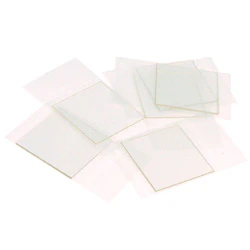
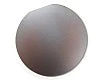
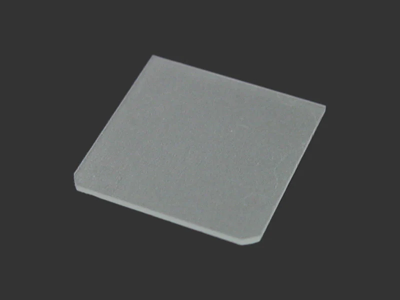
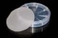
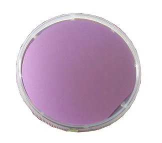
Thermal Oxide Wafer: 50 nm SiO2 Layer on Si (100), 2" dia x 0.30 mm t, N type , undoped, R>1000 ohm-cm
Thermal Oxide Wafer: 50 nm SiO2 Layer on Si (100), 2" dia x 0.30 mm t, N type , undoped, R>1000 ohm-cm
Thermal oxide Layer
-
Research Grade , about 80 % useful area
- SiO2 layer on 2" Silicon wafer
- Oxide layer thickness: 50 nm ( 500A) +/-10%
- Refractive index - 1.455
Silicon Wafer Specifications:
- Conductive type: N- type/ Un- doped
- Resistivity: >1000 ohm-cm
- Size: 50.8 diameter +/- 0.5 mm x 0.3 +/- 0.025 mm
- Orientation: (100) +/- 1o
- Polish: one side polished
- Surface roughnessm, Ra: < 5A(RMS)
Related Products
 |
|
|
|
|
|
Thin Films A-Z |
Crystal wafer A-Z |
Plasma Cleaner |
Wafer Containers |
Dicing saw |
Film Coater |
$119.00
Thermal Oxide Wafer: 50 nm SiO2 Layer on Si (100), 2" dia x 0.30 mm t, N type , undoped, R>1000 ohm-cm—
$119.00
Thermal Oxide Wafer: 50 nm SiO2 Layer on Si (100), 2" dia x 0.30 mm t, N type , undoped, R>1000 ohm-cm
Thermal oxide Layer
-
Research Grade , about 80 % useful area
- SiO2 layer on 2" Silicon wafer
- Oxide layer thickness: 50 nm ( 500A) +/-10%
- Refractive index - 1.455
Silicon Wafer Specifications:
- Conductive type: N- type/ Un- doped
- Resistivity: >1000 ohm-cm
- Size: 50.8 diameter +/- 0.5 mm x 0.3 +/- 0.025 mm
- Orientation: (100) +/- 1o
- Polish: one side polished
- Surface roughnessm, Ra: < 5A(RMS)
Related Products
|
|
|
|
|
|
Thin Films A-Z |
Crystal wafer A-Z |
Plasma Cleaner |
Wafer Containers |
Dicing saw |
Film Coater |
Product Information
Product Information
Shipping & Returns
Shipping & Returns
Description
Thermal oxide Layer
-
Research Grade , about 80 % useful area
- SiO2 layer on 2" Silicon wafer
- Oxide layer thickness: 50 nm ( 500A) +/-10%
- Refractive index - 1.455
Silicon Wafer Specifications:
- Conductive type: N- type/ Un- doped
- Resistivity: >1000 ohm-cm
- Size: 50.8 diameter +/- 0.5 mm x 0.3 +/- 0.025 mm
- Orientation: (100) +/- 1o
- Polish: one side polished
- Surface roughnessm, Ra: < 5A(RMS)
Related Products
|
|
|
|
|
|
Thin Films A-Z |
Crystal wafer A-Z |
Plasma Cleaner |
Wafer Containers |
Dicing saw |
Film Coater |