🚚 Free Worldwide Shipping on All Orders!Shop Now
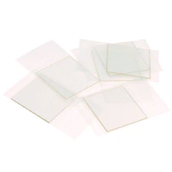
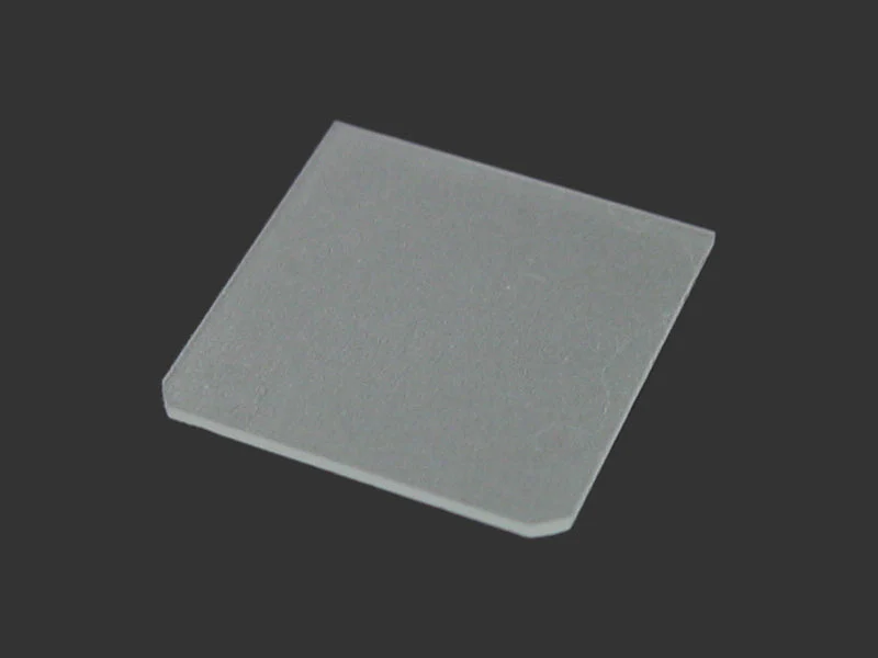
Silicon-on-Sapphire (11-02, R Plane ), 100mm Dia x 0.46mm,1sp, Film: 0.6 um thick
Silicon on sapphire (SOS) is a hetero-epitaxialprocess for integrated circuitmanufacturing that consists of a thin layer (typically thinner than 0.6 micrometres) of silicongrown on a sapphire (Al2O3) wafer. SOS is part of the Silicon on Insulator (SOI) family of CMOS technologies. SOS is primarily used in aerospace and militaryapplications because of its inherent resistance to radiation.
U.S. Dept. of Commerce requires End User Certificate for exporting this product. Oversea end users must file the end user certificate form (click to download) and all sales are subject to get approval by U.S. Dept. of Commerce before shipping.
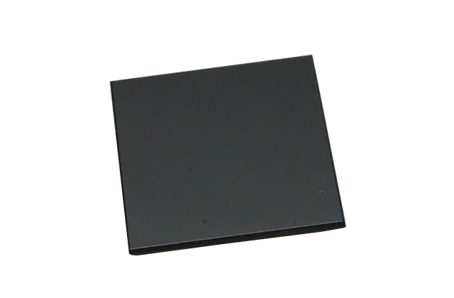
SOS(Silicon on Sapphire) Wafers (DSP-Double sides polished)
Silicon EPI Layer:
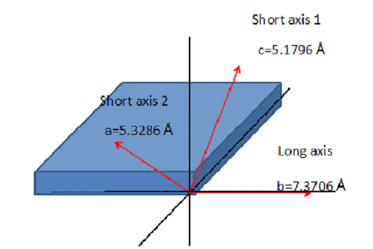
- Silicon Orientation: (100)
- Type, Dopant: Intrinsic type, undoped
- Silicon Thickness: 0.6 um +/- 10%
- Resistivity: > 100 ohm.cm
- Micro-particle density ( for particles > 2 um) < 2/cm^2
Sapphire Wafer:
- R plane -- (1-102) with single flat
Purity: 99.996% - Wafer size: 100 mm dia x 0.46 mm thickness
- Flat : One flat 32.5mm +/-2.5mm, at 45+/- 1 deg CCW from <C> on <R>
- Front surface: Epi-polished (Ra < 4 nm)
- Back surface: Fine ground
- TTV < 15 um, Bow < 20 um, Warp < 20 um, Flatness (TIR) < 12 um, with Laser Mark on wafer back-side, just below the Flat
Related Products
 |
|
|
|
|
|
Thin Films A-Z |
Crystal wafer A-Z |
Plasma Cleaner |
Wafer Containers |
Dicing saw |
Film Coater |
$419.65
Original: $1,199.00
-65%Silicon-on-Sapphire (11-02, R Plane ), 100mm Dia x 0.46mm,1sp, Film: 0.6 um thick—
$1,199.00
$419.65Silicon-on-Sapphire (11-02, R Plane ), 100mm Dia x 0.46mm,1sp, Film: 0.6 um thick
Silicon on sapphire (SOS) is a hetero-epitaxialprocess for integrated circuitmanufacturing that consists of a thin layer (typically thinner than 0.6 micrometres) of silicongrown on a sapphire (Al2O3) wafer. SOS is part of the Silicon on Insulator (SOI) family of CMOS technologies. SOS is primarily used in aerospace and militaryapplications because of its inherent resistance to radiation.
U.S. Dept. of Commerce requires End User Certificate for exporting this product. Oversea end users must file the end user certificate form (click to download) and all sales are subject to get approval by U.S. Dept. of Commerce before shipping.
SOS(Silicon on Sapphire) Wafers (DSP-Double sides polished)
Silicon EPI Layer:
- Silicon Orientation: (100)
- Type, Dopant: Intrinsic type, undoped
- Silicon Thickness: 0.6 um +/- 10%
- Resistivity: > 100 ohm.cm
- Micro-particle density ( for particles > 2 um) < 2/cm^2
Sapphire Wafer:
- R plane -- (1-102) with single flat
Purity: 99.996% - Wafer size: 100 mm dia x 0.46 mm thickness
- Flat : One flat 32.5mm +/-2.5mm, at 45+/- 1 deg CCW from <C> on <R>
- Front surface: Epi-polished (Ra < 4 nm)
- Back surface: Fine ground
- TTV < 15 um, Bow < 20 um, Warp < 20 um, Flatness (TIR) < 12 um, with Laser Mark on wafer back-side, just below the Flat
Related Products
|
|
|
|
|
|
Thin Films A-Z |
Crystal wafer A-Z |
Plasma Cleaner |
Wafer Containers |
Dicing saw |
Film Coater |
Product Information
Product Information
Shipping & Returns
Shipping & Returns
Description
Silicon on sapphire (SOS) is a hetero-epitaxialprocess for integrated circuitmanufacturing that consists of a thin layer (typically thinner than 0.6 micrometres) of silicongrown on a sapphire (Al2O3) wafer. SOS is part of the Silicon on Insulator (SOI) family of CMOS technologies. SOS is primarily used in aerospace and militaryapplications because of its inherent resistance to radiation.
U.S. Dept. of Commerce requires End User Certificate for exporting this product. Oversea end users must file the end user certificate form (click to download) and all sales are subject to get approval by U.S. Dept. of Commerce before shipping.
SOS(Silicon on Sapphire) Wafers (DSP-Double sides polished)
Silicon EPI Layer:
- Silicon Orientation: (100)
- Type, Dopant: Intrinsic type, undoped
- Silicon Thickness: 0.6 um +/- 10%
- Resistivity: > 100 ohm.cm
- Micro-particle density ( for particles > 2 um) < 2/cm^2
Sapphire Wafer:
- R plane -- (1-102) with single flat
Purity: 99.996% - Wafer size: 100 mm dia x 0.46 mm thickness
- Flat : One flat 32.5mm +/-2.5mm, at 45+/- 1 deg CCW from <C> on <R>
- Front surface: Epi-polished (Ra < 4 nm)
- Back surface: Fine ground
- TTV < 15 um, Bow < 20 um, Warp < 20 um, Flatness (TIR) < 12 um, with Laser Mark on wafer back-side, just below the Flat
Related Products
|
|
|
|
|
|
Thin Films A-Z |
Crystal wafer A-Z |
Plasma Cleaner |
Wafer Containers |
Dicing saw |
Film Coater |