🚚 Free Worldwide Shipping on All Orders!Shop Now

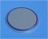
SiO2+Ti+Pt(111) thin film on Si substrate ,2"x0.279mm,1sp P-type B-doped.R:1-20 ohm.cm
Silicon Wafer Specifications:
-
Film: SiO2+Ti+Pt(111) thin film on Si (100) (P-type) substrate ,2"x0.279mm, 1 side polished (1sp)
- SiO2=300 nm
- Ti=10 nm
- Pt(111)=150 nm
- Resistivity: 1-20 ohm.cm (If you would like to measure the resistivity accurately,
please order our Portable 4 Probe Resistivity Testing Instrument.) - Substrate Size: 2" diameter +/- 0.5 mm x 0.279 mm
- Polish: one side polished
- Surface roughness: < 20 A RMS
- Maximum Thermal Budget of Pt film: < 650-700 degree C / 1 hr
- Optional: you may need tool below to handle the wafer ( click picture to order )

$139.65
Original: $399.00
-65%SiO2+Ti+Pt(111) thin film on Si substrate ,2"x0.279mm,1sp P-type B-doped.R:1-20 ohm.cm—
$399.00
$139.65SiO2+Ti+Pt(111) thin film on Si substrate ,2"x0.279mm,1sp P-type B-doped.R:1-20 ohm.cm
Silicon Wafer Specifications:
-
Film: SiO2+Ti+Pt(111) thin film on Si (100) (P-type) substrate ,2"x0.279mm, 1 side polished (1sp)
- SiO2=300 nm
- Ti=10 nm
- Pt(111)=150 nm
- Resistivity: 1-20 ohm.cm (If you would like to measure the resistivity accurately,
please order our Portable 4 Probe Resistivity Testing Instrument.) - Substrate Size: 2" diameter +/- 0.5 mm x 0.279 mm
- Polish: one side polished
- Surface roughness: < 20 A RMS
- Maximum Thermal Budget of Pt film: < 650-700 degree C / 1 hr
- Optional: you may need tool below to handle the wafer ( click picture to order )
Product Information
Product Information
Shipping & Returns
Shipping & Returns
Description
Silicon Wafer Specifications:
-
Film: SiO2+Ti+Pt(111) thin film on Si (100) (P-type) substrate ,2"x0.279mm, 1 side polished (1sp)
- SiO2=300 nm
- Ti=10 nm
- Pt(111)=150 nm
- Resistivity: 1-20 ohm.cm (If you would like to measure the resistivity accurately,
please order our Portable 4 Probe Resistivity Testing Instrument.) - Substrate Size: 2" diameter +/- 0.5 mm x 0.279 mm
- Polish: one side polished
- Surface roughness: < 20 A RMS
- Maximum Thermal Budget of Pt film: < 650-700 degree C / 1 hr
- Optional: you may need tool below to handle the wafer ( click picture to order )