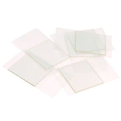
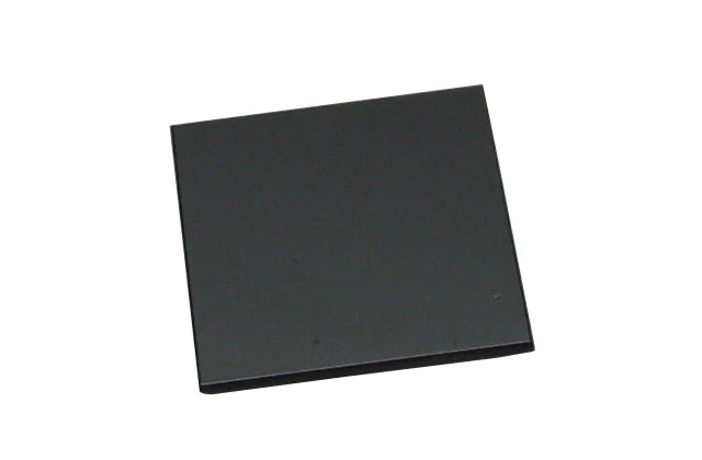
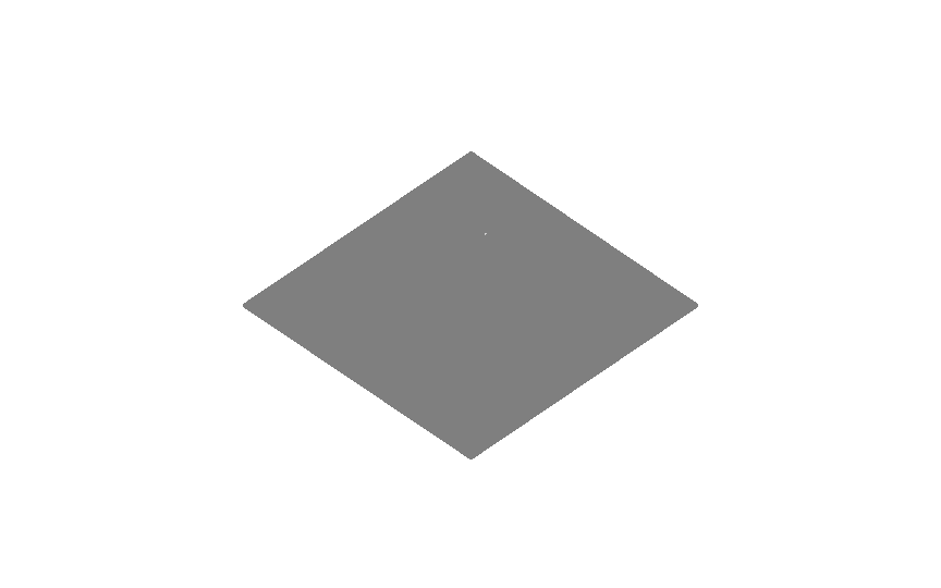
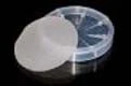
single crystal LaAlO3 wafer, (100), 0.5"x 0.5" x 0.5mm , 2 side polished
|
LaAlO3 single crystal provides a good lattice match to many materials with perovskite structure. It is an excellent substrate for the epitaxial growth of high Tc superconductors and magnetic and ferroelectric thin films. The dielectric properties of LaAlO3 crystal are well-suitable for low-loss microwave and dielectric resonance applications. Substrate Specifications:
| |
Typical Physical Properties |
|
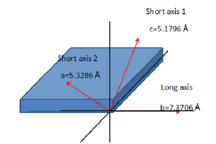
Crystal Structure |
|
Growth Method |
Czochralski |
Density |
6.52 g/cm3 |
Melt Point |
2080 oC |
Thermal expansion |
10 (x10-6/ oC) |
Dielectric Constant |
~ 25 |
Loss Tangent at 10 GHz |
~3x10⁻⁴ @ 300K , ~0.6 x10⁻⁴ @77K |
Color and Appearance |
Transparent to Brown based on annealing condition. |
Chemical Stability |
Insoluble in mineral acids at 25 oC and soluble in H3PO3 at> 150 oC |

Related Products
LSAT |
LaAlO3 |
GGG |
NdCaAlO4 |
YSZ |
SrTiO3 |
|
|
|
|
|
|
SrLaAlO4 |
NdGaO3 |
Crystal A-Z |
Wafer Box |
RTP Furnaces |
Film Coater |
|
|
|
|
|

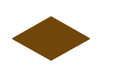
single crystal LaAlO3 wafer, (100), 0.5"x 0.5" x 0.5mm , 2 side polished
|
LaAlO3 single crystal provides a good lattice match to many materials with perovskite structure. It is an excellent substrate for the epitaxial growth of high Tc superconductors and magnetic and ferroelectric thin films. The dielectric properties of LaAlO3 crystal are well-suitable for low-loss microwave and dielectric resonance applications. Substrate Specifications:
| |
Typical Physical Properties |
|
Crystal Structure |
|
Growth Method |
Czochralski |
Density |
6.52 g/cm3 |
Melt Point |
2080 oC |
Thermal expansion |
10 (x10-6/ oC) |
Dielectric Constant |
~ 25 |
Loss Tangent at 10 GHz |
~3x10⁻⁴ @ 300K , ~0.6 x10⁻⁴ @77K |
Color and Appearance |
Transparent to Brown based on annealing condition. |
Chemical Stability |
Insoluble in mineral acids at 25 oC and soluble in H3PO3 at> 150 oC |
Related Products
LSAT |
LaAlO3 |
GGG |
NdCaAlO4 |
YSZ |
SrTiO3 |
|
|
|
|
|
|
SrLaAlO4 |
NdGaO3 |
Crystal A-Z |
Wafer Box |
RTP Furnaces |
Film Coater |
|
|
|
|
|
Product Information
Product Information
Shipping & Returns
Shipping & Returns
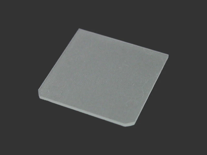
Description
|
LaAlO3 single crystal provides a good lattice match to many materials with perovskite structure. It is an excellent substrate for the epitaxial growth of high Tc superconductors and magnetic and ferroelectric thin films. The dielectric properties of LaAlO3 crystal are well-suitable for low-loss microwave and dielectric resonance applications. Substrate Specifications:
| |
Typical Physical Properties |
|
Crystal Structure |
|
Growth Method |
Czochralski |
Density |
6.52 g/cm3 |
Melt Point |
2080 oC |
Thermal expansion |
10 (x10-6/ oC) |
Dielectric Constant |
~ 25 |
Loss Tangent at 10 GHz |
~3x10⁻⁴ @ 300K , ~0.6 x10⁻⁴ @77K |
Color and Appearance |
Transparent to Brown based on annealing condition. |
Chemical Stability |
Insoluble in mineral acids at 25 oC and soluble in H3PO3 at> 150 oC |
Related Products
LSAT |
LaAlO3 |
GGG |
NdCaAlO4 |
YSZ |
SrTiO3 |
|
|
|
|
|
|
SrLaAlO4 |
NdGaO3 |
Crystal A-Z |
Wafer Box |
RTP Furnaces |
Film Coater |
|
|
|
|
|