🚚 Free Worldwide Shipping on All Orders!Shop Now

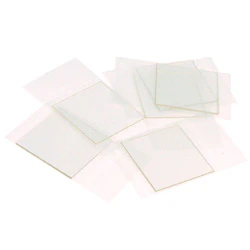
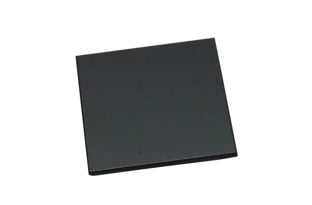
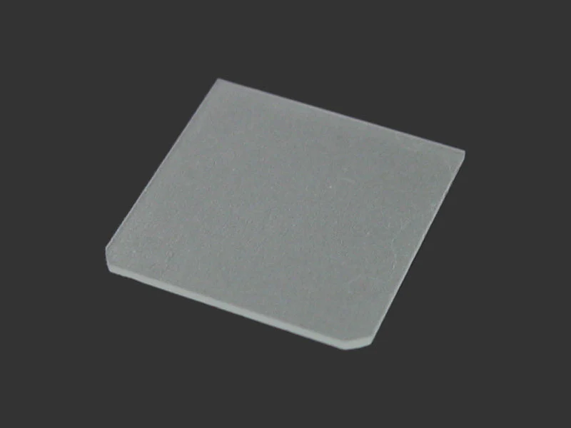
SiC - 4H (0001), 5x5x0.3 mm , one side polished ( C side)
Specifications of Substrate
- Orientation: <0001> +/-0.5
- Dimension: 5x5 x 0.3 +/-0.03 mm
- Polished: One sides epi polished on C face
- Surface Roughness: < 10 A by AFM
Typical Properties of Single Crystal SiC
- Formula weight: 40.10
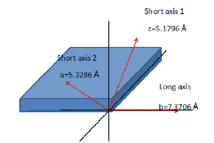
- Unit Cell: Hexagonal
- Lattice constant: a =3.07 A c = 10.05 A
- Stacking sequence: ABCB (4H)
- Growth Technique: MOCVD
- Polishing : Silicon face polished
- Band Gap: 3.26 eV ( Indirect)
- Conductivity type: N
- TTV/Bow/Warp: <=35um
- Micropipe Density: <=30 cm^-2
- Resistivity: 0.01~0.5 ohm-cm
- Dielectric Constant: e (11) = e (22) = 9.66 e (33) = 10.33
- Thermal Conductivity @ 300K: 4 W / cm . K
- Hardness: 9 Mohs
- Doping level of nitrogen atoms : 10^18-19 cm^-3
Related Product
|
Other SiC |
GaN |
AlN template |
ZnO |
|
|
|
|
|
|
Sapphire |
Dicing Saw |
Wafer Containers |
Film Coater |
|
|
|
|
$12.58
Original: $35.95
-65%SiC - 4H (0001), 5x5x0.3 mm , one side polished ( C side)—
$35.95
$12.58SiC - 4H (0001), 5x5x0.3 mm , one side polished ( C side)
Specifications of Substrate
- Orientation: <0001> +/-0.5
- Dimension: 5x5 x 0.3 +/-0.03 mm
- Polished: One sides epi polished on C face
- Surface Roughness: < 10 A by AFM
Typical Properties of Single Crystal SiC
- Formula weight: 40.10
- Unit Cell: Hexagonal
- Lattice constant: a =3.07 A c = 10.05 A
- Stacking sequence: ABCB (4H)
- Growth Technique: MOCVD
- Polishing : Silicon face polished
- Band Gap: 3.26 eV ( Indirect)
- Conductivity type: N
- TTV/Bow/Warp: <=35um
- Micropipe Density: <=30 cm^-2
- Resistivity: 0.01~0.5 ohm-cm
- Dielectric Constant: e (11) = e (22) = 9.66 e (33) = 10.33
- Thermal Conductivity @ 300K: 4 W / cm . K
- Hardness: 9 Mohs
- Doping level of nitrogen atoms : 10^18-19 cm^-3
Related Product
|
Other SiC |
GaN |
AlN template |
ZnO |
|
|
|
|
|
|
Sapphire |
Dicing Saw |
Wafer Containers |
Film Coater |
|
|
|
|
Product Information
Product Information
Shipping & Returns
Shipping & Returns
Description
Specifications of Substrate
- Orientation: <0001> +/-0.5
- Dimension: 5x5 x 0.3 +/-0.03 mm
- Polished: One sides epi polished on C face
- Surface Roughness: < 10 A by AFM
Typical Properties of Single Crystal SiC
- Formula weight: 40.10
- Unit Cell: Hexagonal
- Lattice constant: a =3.07 A c = 10.05 A
- Stacking sequence: ABCB (4H)
- Growth Technique: MOCVD
- Polishing : Silicon face polished
- Band Gap: 3.26 eV ( Indirect)
- Conductivity type: N
- TTV/Bow/Warp: <=35um
- Micropipe Density: <=30 cm^-2
- Resistivity: 0.01~0.5 ohm-cm
- Dielectric Constant: e (11) = e (22) = 9.66 e (33) = 10.33
- Thermal Conductivity @ 300K: 4 W / cm . K
- Hardness: 9 Mohs
- Doping level of nitrogen atoms : 10^18-19 cm^-3
Related Product
|
Other SiC |
GaN |
AlN template |
ZnO |
|
|
|
|
|
|
Sapphire |
Dicing Saw |
Wafer Containers |
Film Coater |
|
|
|
|