🚚 Free Worldwide Shipping on All Orders!Shop Now

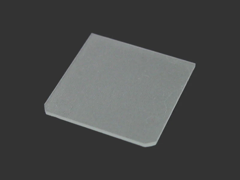
Si Wafer (100), 4 " dia x 0.275 mm, P Type B doped, 1SP, Resistivities: 0.5 - 2.0 ohm-cm
- Single Crystal: Si
- Growth Method: CZ
- Type/Dopant: P/Boron
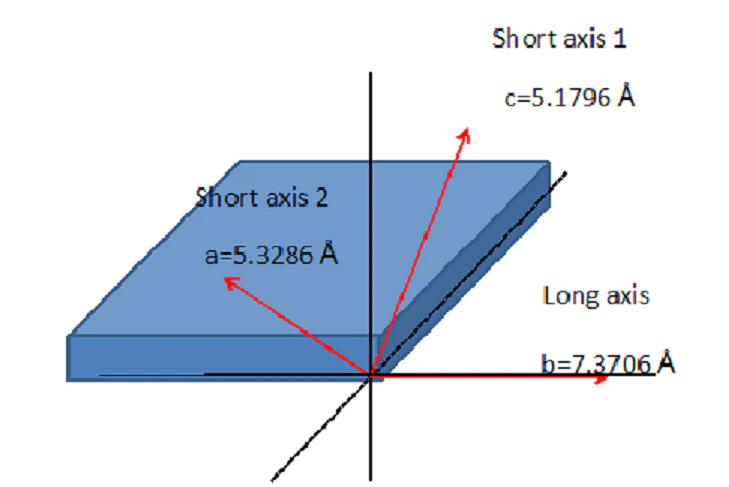
- Orientation: (100)
- Resistivity: 0.5 - 2.0 ohm-cm (If you would like to measure the resistivity accurately,
please order our Portable 4 Probe Resistivity Testing Instrument.) - Diameter: 100 mm
- Thickness: 0.275 mm +/- 0.020 mm
- Primary Flat: <110>
- Polish: One side polished
- Minority-Carrier Lifetime: 100 us
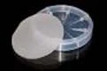
Optional: you may need tool below to handle the wafer ( click picture to order )
|
|
|
|
|
Other Crystal wafer A-Z |
Plasma Cleaner |
Wafer Containers |
Dicing saw |
Film Coater |
$27.65
Original: $79.00
-65%Si Wafer (100), 4 " dia x 0.275 mm, P Type B doped, 1SP, Resistivities: 0.5 - 2.0 ohm-cm—
$79.00
$27.65Si Wafer (100), 4 " dia x 0.275 mm, P Type B doped, 1SP, Resistivities: 0.5 - 2.0 ohm-cm
- Single Crystal: Si
- Growth Method: CZ
- Type/Dopant: P/Boron
- Orientation: (100)
- Resistivity: 0.5 - 2.0 ohm-cm (If you would like to measure the resistivity accurately,
please order our Portable 4 Probe Resistivity Testing Instrument.) - Diameter: 100 mm
- Thickness: 0.275 mm +/- 0.020 mm
- Primary Flat: <110>
- Polish: One side polished
- Minority-Carrier Lifetime: 100 us
Optional: you may need tool below to handle the wafer ( click picture to order )
|
|
|
|
|
Other Crystal wafer A-Z |
Plasma Cleaner |
Wafer Containers |
Dicing saw |
Film Coater |
Product Information
Product Information
Shipping & Returns
Shipping & Returns
Description
- Single Crystal: Si
- Growth Method: CZ
- Type/Dopant: P/Boron
- Orientation: (100)
- Resistivity: 0.5 - 2.0 ohm-cm (If you would like to measure the resistivity accurately,
please order our Portable 4 Probe Resistivity Testing Instrument.) - Diameter: 100 mm
- Thickness: 0.275 mm +/- 0.020 mm
- Primary Flat: <110>
- Polish: One side polished
- Minority-Carrier Lifetime: 100 us
Optional: you may need tool below to handle the wafer ( click picture to order )
|
|
|
|
|
Other Crystal wafer A-Z |
Plasma Cleaner |
Wafer Containers |
Dicing saw |
Film Coater |