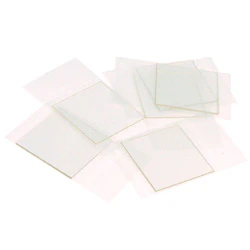
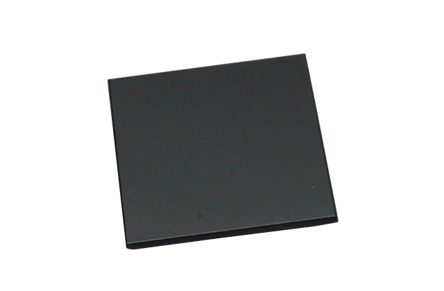
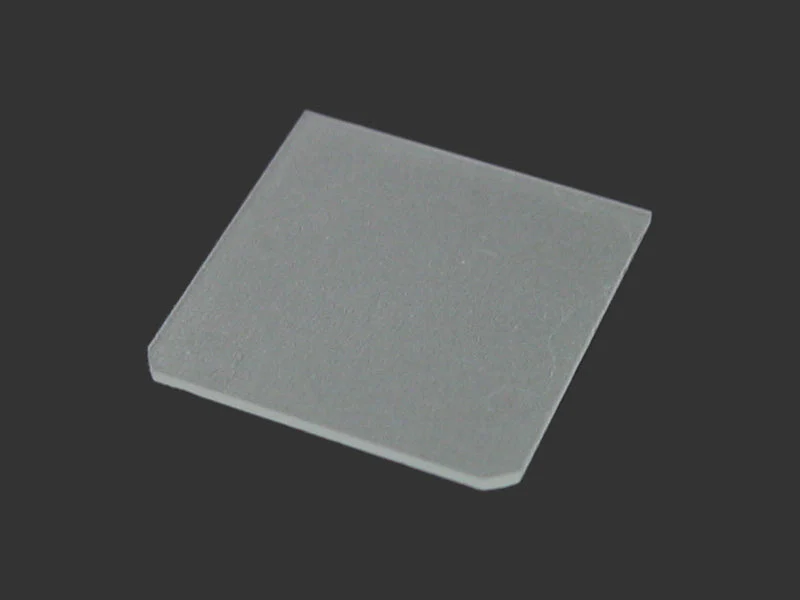
PMNT Substrate (001) 10x10x0.5mm, two sides polished - PMNTb101005S2
Substrate Specifications
- Size: 10x10x 0.5mm +/-0.05mm
-
Orientation: (001 ) +/-0.5 Deg
-
Growing Method: Bridgman method
- Polish: Two sides EPI polished by CMP technology with less sub-surface lattice damage.
- Surface finish ( Ra) : < 10A
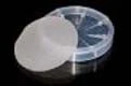
- Pack: Packed in 100 grade plastic bag under 1000 class clean room.
- Warning: PMNT crystal has a visible twin on a polished surface, which is normal nature .
Typical Properties
-
ChemicalComposition:
( PbMg 0.33 Nb 0.67)1-x: (PbTiO3)x; x=0.29-0.32
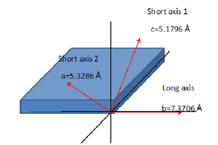
Crystalstructure / Lattice
R3m, Rhombohedral
a0 ~~ 4.024 A, (pseudo-cubic, varies with composition
Melting Point:
1280 oC
Density
8.1 g/cm3
Piezoelectric Coefficient
d33 m >2000 pC/N
Coupling Constant
k33 (longitudinal mode) >92%
kt (thickness mode) 59-62%
k33' (beam mode) 84-88%
Dielectric Constant
e (at 1kHz after poling) 4000
Dielectric loss
tan delta < 0.9
Curie temperature:
135-150 oC
Max size
25 mm x 25 mm x 1- 2 mm thickness along [001],
Related Products
|
LaAlO3 |
MgO |
YSZ |
SrLaAlO4 |
|
|
|
|
|
|
Dicing Saw |
RTP Furnace |
Wafer Containers |
Film Coaters |
|
|
|
|
|
PMNT Substrate (001) 10x10x0.5mm, two sides polished - PMNTb101005S2
Substrate Specifications
- Size: 10x10x 0.5mm +/-0.05mm
-
Orientation: (001 ) +/-0.5 Deg
-
Growing Method: Bridgman method
- Polish: Two sides EPI polished by CMP technology with less sub-surface lattice damage.
- Surface finish ( Ra) : < 10A
- Pack: Packed in 100 grade plastic bag under 1000 class clean room.
- Warning: PMNT crystal has a visible twin on a polished surface, which is normal nature .
Typical Properties
-
ChemicalComposition:
( PbMg 0.33 Nb 0.67)1-x: (PbTiO3)x; x=0.29-0.32
Crystalstructure / Lattice
R3m, Rhombohedral
a0 ~~ 4.024 A, (pseudo-cubic, varies with composition
Melting Point:
1280 oC
Density
8.1 g/cm3
Piezoelectric Coefficient
d33 m >2000 pC/N
Coupling Constant
k33 (longitudinal mode) >92%
kt (thickness mode) 59-62%
k33' (beam mode) 84-88%
Dielectric Constant
e (at 1kHz after poling) 4000
Dielectric loss
tan delta < 0.9
Curie temperature:
135-150 oC
Max size
25 mm x 25 mm x 1- 2 mm thickness along [001],
Related Products
|
LaAlO3 |
MgO |
YSZ |
SrLaAlO4 |
|
|
|
|
|
|
Dicing Saw |
RTP Furnace |
Wafer Containers |
Film Coaters |
|
|
|
|
|
Product Information
Product Information
Shipping & Returns
Shipping & Returns
Description
Substrate Specifications
- Size: 10x10x 0.5mm +/-0.05mm
-
Orientation: (001 ) +/-0.5 Deg
-
Growing Method: Bridgman method
- Polish: Two sides EPI polished by CMP technology with less sub-surface lattice damage.
- Surface finish ( Ra) : < 10A
- Pack: Packed in 100 grade plastic bag under 1000 class clean room.
- Warning: PMNT crystal has a visible twin on a polished surface, which is normal nature .
Typical Properties
-
ChemicalComposition:
( PbMg 0.33 Nb 0.67)1-x: (PbTiO3)x; x=0.29-0.32
Crystalstructure / Lattice
R3m, Rhombohedral
a0 ~~ 4.024 A, (pseudo-cubic, varies with composition
Melting Point:
1280 oC
Density
8.1 g/cm3
Piezoelectric Coefficient
d33 m >2000 pC/N
Coupling Constant
k33 (longitudinal mode) >92%
kt (thickness mode) 59-62%
k33' (beam mode) 84-88%
Dielectric Constant
e (at 1kHz after poling) 4000
Dielectric loss
tan delta < 0.9
Curie temperature:
135-150 oC
Max size
25 mm x 25 mm x 1- 2 mm thickness along [001],
Related Products
|
LaAlO3 |
MgO |
YSZ |
SrLaAlO4 |
|
|
|
|
|
|
Dicing Saw |
RTP Furnace |
Wafer Containers |
Film Coaters |
|
|
|
|
|