🚚 Free Worldwide Shipping on All Orders!Shop Now

HomeStore
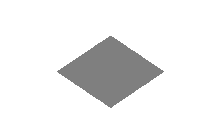
Nickel<111> Film (100nm) Coated SiO2/Si Wafer -(100) P/Boron ,10x10x0.5mmSSP, R:1-20 ohm.cm - Ni-SO/Si-101005S1
Nickel<111> Film (100nm) Coated SiO2/Si Wafer -(100) P/Boron ,10x10x0.5mmSSP, R:1-20 ohm.cm - Ni-SO/Si-101005S1
Nickel Film
- Nickel Film Thickness: 100nm
- Film Crystallinity: (111) - oriented polycrystals
Silicon Wafer Specifications:
- Conductive type: Si P- type, B-doped
- Resistivity: 1-20 ohm-cm
- Size: 10x10x0.5mm
- SiO2 Thichness: 300 nm
- Orientation: (100) +/- 0.5o
- Polish: One sides polished
- Surface roughness: Prime
- Packing: Vacuum packed on a 4" single wafer carrier
- Optional: you may need tool below to handle the wafer ( click picture to order )
Related Products
|
|
|
|
|
|
Thin Films A-Z |
Crystal wafer A-Z |
Plasma Cleaner |
Wafer Containers |
Dicing saw |
Film Coater |
$98.00
Nickel<111> Film (100nm) Coated SiO2/Si Wafer -(100) P/Boron ,10x10x0.5mmSSP, R:1-20 ohm.cm - Ni-SO/Si-101005S1—
$98.00
Nickel<111> Film (100nm) Coated SiO2/Si Wafer -(100) P/Boron ,10x10x0.5mmSSP, R:1-20 ohm.cm - Ni-SO/Si-101005S1
Nickel Film
- Nickel Film Thickness: 100nm
- Film Crystallinity: (111) - oriented polycrystals
Silicon Wafer Specifications:
- Conductive type: Si P- type, B-doped
- Resistivity: 1-20 ohm-cm
- Size: 10x10x0.5mm
- SiO2 Thichness: 300 nm
- Orientation: (100) +/- 0.5o
- Polish: One sides polished
- Surface roughness: Prime
- Packing: Vacuum packed on a 4" single wafer carrier
- Optional: you may need tool below to handle the wafer ( click picture to order )
Related Products
|
|
|
|
|
|
Thin Films A-Z |
Crystal wafer A-Z |
Plasma Cleaner |
Wafer Containers |
Dicing saw |
Film Coater |
Product Information
Product Information
Shipping & Returns
Shipping & Returns
Description
Nickel Film
- Nickel Film Thickness: 100nm
- Film Crystallinity: (111) - oriented polycrystals
Silicon Wafer Specifications:
- Conductive type: Si P- type, B-doped
- Resistivity: 1-20 ohm-cm
- Size: 10x10x0.5mm
- SiO2 Thichness: 300 nm
- Orientation: (100) +/- 0.5o
- Polish: One sides polished
- Surface roughness: Prime
- Packing: Vacuum packed on a 4" single wafer carrier
- Optional: you may need tool below to handle the wafer ( click picture to order )
Related Products
|
|
|
|
|
|
Thin Films A-Z |
Crystal wafer A-Z |
Plasma Cleaner |
Wafer Containers |
Dicing saw |
Film Coater |