GdScO3 (001)10x10x0.5mm 1sp - GSOb101005S1US
- Size: 10mm x 10mm x 0.5mm
- Orientation: (001) + / - 0.5 o
- Edge direction: <110> with notches
- Polish: one side EPI polished with surface roughness Ra< 5 A ( measured by AFM 5x5 μ area)
- Package: one 1000 class clean room with 100 class plastic bag
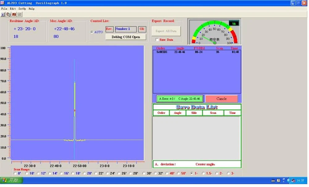
- Typical XRD -rocking curve and AFM curve ( Click Pics below to enlarge )
 XRD-rocking curve
  AFM
AFM
- Good lattice matches with perovskite structure superconductors
- Perfect for ferroelectric epitaxial thin film
- The above single crystals are extremely difficult to grow due to the ultra-high melting point. Nobody can promise each substrate has no defects such as domain, dislocation, and twins If your application is very sensitive to the defects, you must check the substrate by XRD before growing film. MTI will replace the unsatisfied substrate which has no film grown and no damage at free of charge until you are satisfied. No order cancelation is accepted.
Crystal |
Structure /Lattice Constant(A) |
MP oC |
Density (g/cm3) |
Growth Tech |
DyScO3 |
Orthorombic a=5.44 b=5.71 c=7.89 |
2127 |
6.9 |
CZ |
GdScO3 |
Orthorombic a=5.45 b=5.75 c=7.93 |
2127 |
66 |
CZ |
TbScO3 |
Orthorombic |
2127 |
66 |
CZ |
Related Products
|
|
|
|
|
Other Crystal wafers A-Z |
Plasma Cleaner |
Wafer Containers |
Dicing Saw |
Film Coater |
Original: $565.00
-65%$565.00
$197.75GdScO3 (001)10x10x0.5mm 1sp - GSOb101005S1US
- Size: 10mm x 10mm x 0.5mm
- Orientation: (001) + / - 0.5 o
- Edge direction: <110> with notches
- Polish: one side EPI polished with surface roughness Ra< 5 A ( measured by AFM 5x5 μ area)
- Package: one 1000 class clean room with 100 class plastic bag
- Typical XRD -rocking curve and AFM curve ( Click Pics below to enlarge )
- XRD-rocking curve AFM
- Good lattice matches with perovskite structure superconductors
- Perfect for ferroelectric epitaxial thin film
- The above single crystals are extremely difficult to grow due to the ultra-high melting point. Nobody can promise each substrate has no defects such as domain, dislocation, and twins If your application is very sensitive to the defects, you must check the substrate by XRD before growing film. MTI will replace the unsatisfied substrate which has no film grown and no damage at free of charge until you are satisfied. No order cancelation is accepted.
Crystal |
Structure /Lattice Constant(A) |
MP oC |
Density (g/cm3) |
Growth Tech |
DyScO3 |
Orthorombic a=5.44 b=5.71 c=7.89 |
2127 |
6.9 |
CZ |
GdScO3 |
Orthorombic a=5.45 b=5.75 c=7.93 |
2127 |
66 |
CZ |
TbScO3 |
Orthorombic |
2127 |
66 |
CZ |
Related Products
|
|
|
|
|
Other Crystal wafers A-Z |
Plasma Cleaner |
Wafer Containers |
Dicing Saw |
Film Coater |
Product Information
Product Information
Shipping & Returns
Shipping & Returns
Description
- Size: 10mm x 10mm x 0.5mm
- Orientation: (001) + / - 0.5 o
- Edge direction: <110> with notches
- Polish: one side EPI polished with surface roughness Ra< 5 A ( measured by AFM 5x5 μ area)
- Package: one 1000 class clean room with 100 class plastic bag
- Typical XRD -rocking curve and AFM curve ( Click Pics below to enlarge )
- XRD-rocking curve AFM
- Good lattice matches with perovskite structure superconductors
- Perfect for ferroelectric epitaxial thin film
- The above single crystals are extremely difficult to grow due to the ultra-high melting point. Nobody can promise each substrate has no defects such as domain, dislocation, and twins If your application is very sensitive to the defects, you must check the substrate by XRD before growing film. MTI will replace the unsatisfied substrate which has no film grown and no damage at free of charge until you are satisfied. No order cancelation is accepted.
Crystal |
Structure /Lattice Constant(A) |
MP oC |
Density (g/cm3) |
Growth Tech |
DyScO3 |
Orthorombic a=5.44 b=5.71 c=7.89 |
2127 |
6.9 |
CZ |
GdScO3 |
Orthorombic a=5.45 b=5.75 c=7.93 |
2127 |
66 |
CZ |
TbScO3 |
Orthorombic |
2127 |
66 |
CZ |
Related Products
|
|
|
|
|
Other Crystal wafers A-Z |
Plasma Cleaner |
Wafer Containers |
Dicing Saw |
Film Coater |