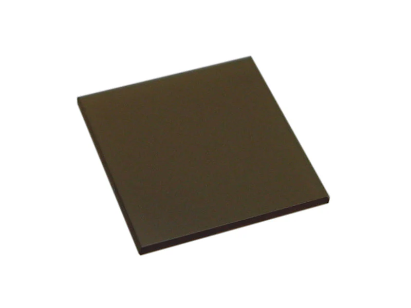
Graphene film on Ni/SiO2/Si 100mm dia,
Graphene™ films are grown directly on a deposited on an oxidized silicon wafer usinga CVD process.
Specifications: Research Grade , about 90 % useful area
- Wafer Size: 100 mm diameter
- Growth Method:Chemical Vapor Deposition (CVD) Technique
-
Film thickness: 1-10 monolayer thick
-
Graphene film is multilayer with thickness varying in the range 1-10 layers;
-
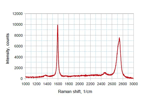
Graphene layers are aligned relative to each (graphite-like A-B stacking ) other as indicated by the Raman spectrum
-
The graphene is grown on Ni film by CVD process.
-
Nickel film is deposited on the substrate covered by thermally grown oxide layer
-
Thickness of the Ni layer is 400 nm;
-
The thickness of the silicon oxide layer is 500 nm;
-
The thickness of the wafer is 500 μm
-
The crystallographic orientation of silicon is 100;
-
-
films are continuous with low defect density.
-
Atomically thin carbon film ( 1-10 layer )
-
Outstanding electronic properties
-
Chemical inertness and stability
-
Unprecedented mechanical strength
 Graphene film structure: three film
graphene film thickness varis from 1 - 10 layer carbon
|
 Optical microstructure picture
|
 Ramam Spectrum
|
Related Products
 |
|
|
|
|
|
|
Thin Films A-Z |
Crystal wafer A-Z |
Plasma Cleaner |
Wafer Containers |
Dicing saw |
Film Coater |
Original: $699.00
-65%$699.00
$244.65More Images
Graphene film on Ni/SiO2/Si 100mm dia,
Graphene™ films are grown directly on a deposited on an oxidized silicon wafer usinga CVD process.
Specifications: Research Grade , about 90 % useful area
- Wafer Size: 100 mm diameter
- Growth Method:Chemical Vapor Deposition (CVD) Technique
-
Film thickness: 1-10 monolayer thick
-
Graphene film is multilayer with thickness varying in the range 1-10 layers;
-
Graphene layers are aligned relative to each (graphite-like A-B stacking ) other as indicated by the Raman spectrum
-
The graphene is grown on Ni film by CVD process.
-
Nickel film is deposited on the substrate covered by thermally grown oxide layer
-
Thickness of the Ni layer is 400 nm;
-
The thickness of the silicon oxide layer is 500 nm;
-
The thickness of the wafer is 500 μm
-
The crystallographic orientation of silicon is 100;
-
-
films are continuous with low defect density.
-
Atomically thin carbon film ( 1-10 layer )
-
Outstanding electronic properties
-
Chemical inertness and stability
-
Unprecedented mechanical strength
|
Graphene film structure: three film
graphene film thickness varis from 1 - 10 layer carbon
|
Optical microstructure picture
|
Ramam Spectrum
|
Related Products
|
|
|
|
|
|
|
Thin Films A-Z |
Crystal wafer A-Z |
Plasma Cleaner |
Wafer Containers |
Dicing saw |
Film Coater |
Product Information
Product Information
Shipping & Returns
Shipping & Returns
Description
Graphene™ films are grown directly on a deposited on an oxidized silicon wafer usinga CVD process.
Specifications: Research Grade , about 90 % useful area
- Wafer Size: 100 mm diameter
- Growth Method:Chemical Vapor Deposition (CVD) Technique
-
Film thickness: 1-10 monolayer thick
-
Graphene film is multilayer with thickness varying in the range 1-10 layers;
-
Graphene layers are aligned relative to each (graphite-like A-B stacking ) other as indicated by the Raman spectrum
-
The graphene is grown on Ni film by CVD process.
-
Nickel film is deposited on the substrate covered by thermally grown oxide layer
-
Thickness of the Ni layer is 400 nm;
-
The thickness of the silicon oxide layer is 500 nm;
-
The thickness of the wafer is 500 μm
-
The crystallographic orientation of silicon is 100;
-
-
films are continuous with low defect density.
-
Atomically thin carbon film ( 1-10 layer )
-
Outstanding electronic properties
-
Chemical inertness and stability
-
Unprecedented mechanical strength
|
Graphene film structure: three film
graphene film thickness varis from 1 - 10 layer carbon
|
Optical microstructure picture
|
Ramam Spectrum
|
Related Products
|
|
|
|
|
|
|
Thin Films A-Z |
Crystal wafer A-Z |
Plasma Cleaner |
Wafer Containers |
Dicing saw |
Film Coater |