🚚 Free Worldwide Shipping on All Orders!Shop Now

HomeStore
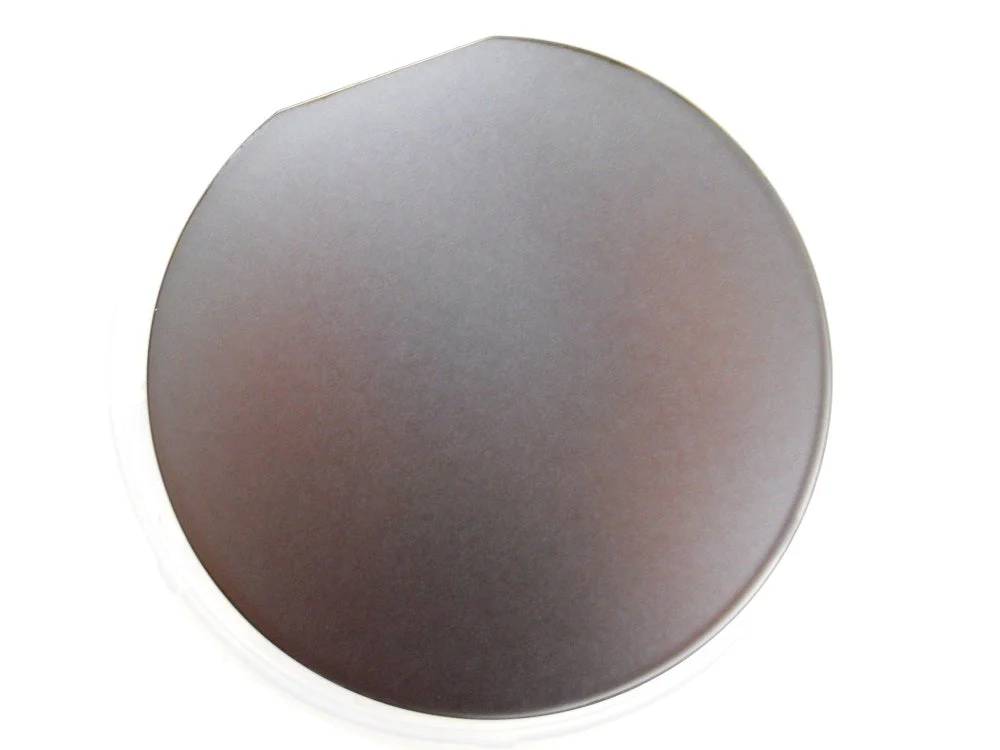
Cu Film on Ta/SiO2/ 4"Silicon Wafer, Cu=100 nm Ta=50nm SiO2=300nm, Si(100) P-type B-doped 4"x0.525mm, 1sp
Cu Film on Ta/SiO2/ 4"Silicon Wafer, Cu=100 nm Ta=50nm SiO2=300nm, Si(100) P-type B-doped 4"x0.525mm, 1sp
Specifications:
- Cu coated SiO2/Si Wafer (4 inch size)
- Thickness of Cu polycrystalline <111> film: 100 nm
- Thickness of Ta diffusion barrier: 50 nm
- 4 inch dia SiO2/ Si wafer (Prime Grade)
- P type, B doped, <100> orientation, Singe side polished
- Resistivities: 1-20 ohm-cm
- thermal oxide: 300 nm thickness
- Surface Roughness: as grown
- Package: One 1000 class clean room with 100 class plastic bag
Related Products
 |
|
iO2 |
|
|
|
Thin Films A-Z |
Crystal wafer A-Z |
Plasma Cleaner |
Wafer Containers |
Dicing saw |
Film Coater |
$599.00
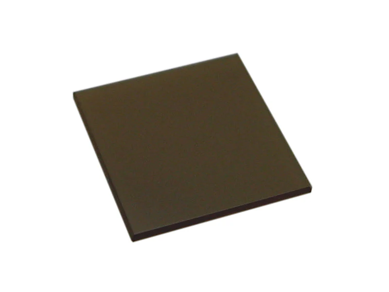
Cu Film on Ta/SiO2/ 4"Silicon Wafer, Cu=100 nm Ta=50nm SiO2=300nm, Si(100) P-type B-doped 4"x0.525mm, 1sp—
$599.00
Cu Film on Ta/SiO2/ 4"Silicon Wafer, Cu=100 nm Ta=50nm SiO2=300nm, Si(100) P-type B-doped 4"x0.525mm, 1sp
Specifications:
- Cu coated SiO2/Si Wafer (4 inch size)
- Thickness of Cu polycrystalline <111> film: 100 nm
- Thickness of Ta diffusion barrier: 50 nm
- 4 inch dia SiO2/ Si wafer (Prime Grade)
- P type, B doped, <100> orientation, Singe side polished
- Resistivities: 1-20 ohm-cm
- thermal oxide: 300 nm thickness
- Surface Roughness: as grown
- Package: One 1000 class clean room with 100 class plastic bag
Related Products
|
|
iO2 |
|
|
|
Thin Films A-Z |
Crystal wafer A-Z |
Plasma Cleaner |
Wafer Containers |
Dicing saw |
Film Coater |
Product Information
Product Information
Shipping & Returns
Shipping & Returns
Description
Specifications:
- Cu coated SiO2/Si Wafer (4 inch size)
- Thickness of Cu polycrystalline <111> film: 100 nm
- Thickness of Ta diffusion barrier: 50 nm
- 4 inch dia SiO2/ Si wafer (Prime Grade)
- P type, B doped, <100> orientation, Singe side polished
- Resistivities: 1-20 ohm-cm
- thermal oxide: 300 nm thickness
- Surface Roughness: as grown
- Package: One 1000 class clean room with 100 class plastic bag
Related Products
|
|
iO2 |
|
|
|
Thin Films A-Z |
Crystal wafer A-Z |
Plasma Cleaner |
Wafer Containers |
Dicing saw |
Film Coater |