🚚 Free Worldwide Shipping on All Orders!Shop Now
HomeStore
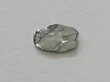
Bi2Te3 Highly Oriented Crystal Substrate (0001) irregular shape(about 10x10x0.1 mm) as Cleaved
Bi2Te3 Highly Oriented Crystal Substrate (0001) irregular shape(about 10x10x0.1 mm) as Cleaved
Bismuth telluride crystal substrate is highly oriented crystal ( not single crystal ), which is a narrow gap layered semiconductor with a hexagonal structure. The valence and conduction band structure can be described as a many-ellipsoidal model with 6 constant-energy ellipsoids that are centered on the reflection planes. General thermoelectric materials, thermoelectric factor is currently the largest pure-phase block; mechanical dissociation can get high-quality topological insulator material.
Specifications:
- Structure: Hexagonal, group 166R-3M
- Grown Method : High-pressure vertical Bridgman
- Lattice constant: a=4.38A c=30.5A
- Substrate orientation: highly oriented layer structure along <0001>
- Surface: as Cleavaged
- Purity: 99.999%, atomic ratio
- Melting Point: 585 oC
- Resistivity : 0.1-5 mohm. cm
- Mobility : 3000 cm2 / V.s
-
General Size: irregular shape(~ 10 mm x 10 mm x 0.1mm)
- Packing: packed in plastic bag with vacuum
Related Products
|
|
|
|
|
Other Crystal wafer A-Z |
Plasma Cleaner |
Wafer Containers |
Dicing saw |
Film Coater |
$488.25
Original: $1,395.00
-65%Bi2Te3 Highly Oriented Crystal Substrate (0001) irregular shape(about 10x10x0.1 mm) as Cleaved—
$1,395.00
$488.25Bi2Te3 Highly Oriented Crystal Substrate (0001) irregular shape(about 10x10x0.1 mm) as Cleaved
Bismuth telluride crystal substrate is highly oriented crystal ( not single crystal ), which is a narrow gap layered semiconductor with a hexagonal structure. The valence and conduction band structure can be described as a many-ellipsoidal model with 6 constant-energy ellipsoids that are centered on the reflection planes. General thermoelectric materials, thermoelectric factor is currently the largest pure-phase block; mechanical dissociation can get high-quality topological insulator material.
Specifications:
- Structure: Hexagonal, group 166R-3M
- Grown Method : High-pressure vertical Bridgman
- Lattice constant: a=4.38A c=30.5A
- Substrate orientation: highly oriented layer structure along <0001>
- Surface: as Cleavaged
- Purity: 99.999%, atomic ratio
- Melting Point: 585 oC
- Resistivity : 0.1-5 mohm. cm
- Mobility : 3000 cm2 / V.s
-
General Size: irregular shape(~ 10 mm x 10 mm x 0.1mm)
- Packing: packed in plastic bag with vacuum
Related Products
|
|
|
|
|
Other Crystal wafer A-Z |
Plasma Cleaner |
Wafer Containers |
Dicing saw |
Film Coater |
Product Information
Product Information
Shipping & Returns
Shipping & Returns
Description
Bismuth telluride crystal substrate is highly oriented crystal ( not single crystal ), which is a narrow gap layered semiconductor with a hexagonal structure. The valence and conduction band structure can be described as a many-ellipsoidal model with 6 constant-energy ellipsoids that are centered on the reflection planes. General thermoelectric materials, thermoelectric factor is currently the largest pure-phase block; mechanical dissociation can get high-quality topological insulator material.
Specifications:
- Structure: Hexagonal, group 166R-3M
- Grown Method : High-pressure vertical Bridgman
- Lattice constant: a=4.38A c=30.5A
- Substrate orientation: highly oriented layer structure along <0001>
- Surface: as Cleavaged
- Purity: 99.999%, atomic ratio
- Melting Point: 585 oC
- Resistivity : 0.1-5 mohm. cm
- Mobility : 3000 cm2 / V.s
-
General Size: irregular shape(~ 10 mm x 10 mm x 0.1mm)
- Packing: packed in plastic bag with vacuum
Related Products
|
|
|
|
|
Other Crystal wafer A-Z |
Plasma Cleaner |
Wafer Containers |
Dicing saw |
Film Coater |
