🚚 Free Worldwide Shipping on All Orders!Shop Now
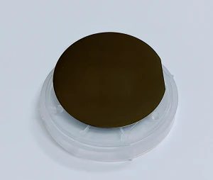
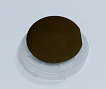
InSb (100) 2" dia x 0.5 mm, N type Undoped, 2 sides polished
2" InSb wafer (N type, Undoped )
- Size: 2" dia x 0.5 (+/- 0.025 ) mm thick
- Orientation: <100> +/-0.5 o
- Type/dopant: N-type/ Undoped
- Surface Polishing : In(A) face polished chemical ,final face
Please click here to see which side is In(A) Face
- Mobility: > 3.9E4 /cm^2/V.S
- EPD: < 200
- Carrier Concentration: (2-7)E14 cm-3@77K
- Growth Method: LEC
- Packing: Sealed in nitrogen in single wafer container at 100 class clean room
$1,650.00
InSb (100) 2" dia x 0.5 mm, N type Undoped, 2 sides polished—
$1,650.00
InSb (100) 2" dia x 0.5 mm, N type Undoped, 2 sides polished
2" InSb wafer (N type, Undoped )
- Size: 2" dia x 0.5 (+/- 0.025 ) mm thick
- Orientation: <100> +/-0.5 o
- Type/dopant: N-type/ Undoped
- Surface Polishing : In(A) face polished chemical ,final face
Please click here to see which side is In(A) Face
- Mobility: > 3.9E4 /cm^2/V.S
- EPD: < 200
- Carrier Concentration: (2-7)E14 cm-3@77K
- Growth Method: LEC
- Packing: Sealed in nitrogen in single wafer container at 100 class clean room
Product Information
Product Information
Shipping & Returns
Shipping & Returns
Description
2" InSb wafer (N type, Undoped )
- Size: 2" dia x 0.5 (+/- 0.025 ) mm thick
- Orientation: <100> +/-0.5 o
- Type/dopant: N-type/ Undoped
- Surface Polishing : In(A) face polished chemical ,final face
Please click here to see which side is In(A) Face
- Mobility: > 3.9E4 /cm^2/V.S
- EPD: < 200
- Carrier Concentration: (2-7)E14 cm-3@77K
- Growth Method: LEC
- Packing: Sealed in nitrogen in single wafer container at 100 class clean room